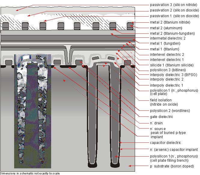
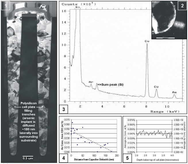
| 
                       
                        
                        The feasibility of using EDX in a FEG TEM to measure the arsenic dopant concentration in a 
                        modern semiconductor device was examined and the results obtained were compared with those 
                        from traditional SIMS dopant concentration profiling techniques.  Using a FEG TEM it is 
                        possible to measure arsenic concentrations down to 0.01 at %(0.025 wt. %) with a lateral 
                        resolution of a few nanometers.
                        
                       
                         A schematic view of a trench cell structure is shown at left, with a FIB/TEM image of the cells superimposed.
                        
                      |