 |
 |
|
About Us
|
 |
 |
 |
 |
|
Fibics Incorporated is a privately owned company specializing in materials science and semiconductor focused ion beam (FIB) applications and analytical services.
Our services include:
Fibics' experienced staff and state-of-the-art analytical instruments mean that we can provide you with solutions that meet your semiconductor or materials science needs at competitive prices and with timely results.
Founded in 1996, we operate from the campus of the Canadian Government's Materials Technology Laboratory (MTL), which gives us access to a host of additional analytical equipment and expertise that our trained operators can use when solving your problems.
Extensive High-End Analytical Equipment and Experience
Strong Links to the Semiconductor Community
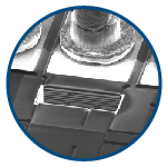
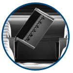
We provide over 2,000 hours of circuit edit / device modification ("microsurgery") to our clients every year, all with fast turnaround, and working on all metal levels of the latest technologies. We also spend hundreds of hours each year on optimization of our techniques and keeping abreast of the latest developments in the field.
Familiarity with State-of-the-art Semiconductor Devices
We prepare & analyze TEM samples from dozens of manufacturers (in Si, GaAs, InP, InGaAsP, GaN, SOS, SOI, etc.), and perform microsurgery on 7 metal, 0.15 um technology devices fabricated at international locations.
Excellent Links to Industrial Materials Science Clients
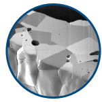
We are a leader in the field of FIB applications to materials science, particularly with regard to TEM specimen preparation to solve complex metallurgical problems. We have extensive experience working with U.S. and European government agencies and research labs, as well as large industrial companies - particularly in the fields of advanced materials and corrosion of a range of metallurgical systems.
History of R&D, Applications Development & Partnerships
Fibics recently developed and sold technology (patent pending) for uniform milling of Copper Interconnect during microsurgery. Fibics has a keen interest in the history of developing novel applications, either under confidentiality agreements or for the purpose of publishing research results to expand the FIB field.
90% of our work is in the field of "real-world, commercial problems." Our work focuses mainly on industrially relevant problems and solutions. Concurrently, we maintain a very strong R&D program.
Please contact us if you have further questions.
|
|