Parallel lapping consists of mounting a de-packaged device or portion of a
device face down on a rotating disk of very fine abrasives (frequently
sub-micron diamond particles) and rotating both the device and abrasive disk
while applying a controlled pressure, slowly lapping ("gently grinding")
away the exposed surface of the device. Carefully designed mounts keep the
lapping uniform over a large area, exposing equivalent levels of the device
in parallel.
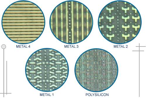
The most common application of parallel lapping is for I.C. delayering, but it can also be used to thin PCBs, compound
semiconductors and a variety of other materials. Parallel lapping of integrated circuits is primarily used for failure analysis and as a
preparation for
FIB deposited probe pads.