Deep sub-micron technologies can pose a problem for
conventional electrical probing - obtaining good physical
contact between a probe and sub-micron circuitry is a
difficult task. To simplify things, a FIB can open probe
windows in the appropriate geometries to make positioning
electrical probes straightforward, as shown in this optical
micrograph.
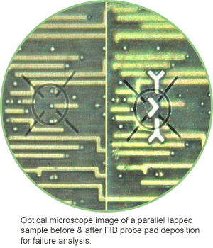
To the right are images of a semiconductor device before and after probe pads, deposited by the FIB, were formed on its surface.
The device was
parallel lapped to expose the vias between the appropriate metal layers, and then the FIB was used to deposit
conductive tungsten in the required geometries on top of the native
dielectric layers of the device.