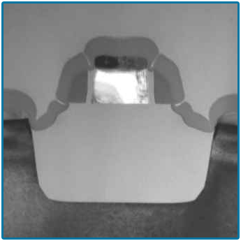
FIB can be used to make site-specific TEM specimens with sub-micron
positional accuracy, using either the conventional
"H-bar" method,
creating large thin areas and iterative thinning, or the new
"lift-out" technique,
which requires no pre-thinning and as a result has a faster turn-around time.
Both techniques can make TEM membranes thin enough for EDX analysis,
EELS analysis,
diffraction patterns, and lattice imaging, not only in
silicon, but in compound semiconductors and many other material systems.
We can also leave the specimen slightly thicker for good
absorption contrast (i.e. visually differentiate oxide and
nitride layers) or dislocation observation!